CHIP GM877C FOR CONVERTING MIPI TO LVDS REFERENCE
1. Requirement
-
Takoyaki uses LVDS panel, only support interfaces TTL and MIPI.
-
Select the peripheral GM877C to convert mipi2 and lvds according to requirements, and indirectly use LVDS panel by this way.
-
Customer A requires lvds panel with a resolution of 960X1280.
-
Customer B requires lvds panel with a resolution of 1920X1080.
2. PUBLIC VERSION STATE
-
The public mi panel owner has lighted up lvds panel with GM877C, and the base code was remained.
-
Customer feedback has no effect on the corresponding panel parameters.
-
Analyze the specific state based on specific problem.
3. Debugging
-
Hardware connection

-
Debugging process
-
First of all, it is necessary to use the GM877C chip aside the main chip to light up the lvds panel to make sure they are OK, what requires hardware engineer to reserve GM's I2C interface and external crystal interface for the board during the initial design.
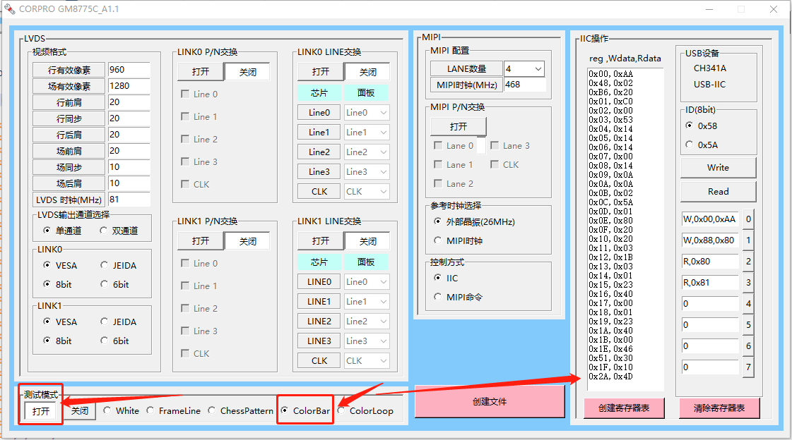
Customer can ask GM manufacturer to cooperate with debugging, the following tool is used. When GM debugs the PC, the tool can automatically generate parameters, and write the GM chip through USB2IIC to light up the LVDS panel.
Note for actual debugging process:
After writing, verify whether the writing is correct through read. If no, through the independent commands
w, 0xxx, 0xxxx, and useR, 0xxxto confirm whether correct. If that is ok, the failure of previous method may be caused by the fast I2C speed, which can be solved by manually writing individually one by one, and check by reading.
-
After lighting the panel according to the above, it is roughly confirmed that the GM+panel circuit is correct, and LVDS panel parameter is ok. Use the GM tool to switch to "MIPI command", and add the generation command parameters to GM8775C_CMD. Note: At the beginning, it is recommended to open the test pattern for the generation test command, as follows:

-
Modify stPanelParam and fill in according to panel spec.
MI_PANEL_ParamConfig_t stPanelParam =
{
"GM8775C_960x1280", //const char *pPanelName; ///< PanelName
0, //MI_U8 MI_U8Dither; ///< Diether On?off
E_MI_PNL_LINK_MIPI_DSI, //MIPnlLinkType_e eLinkType; ///< Panel LinkType
0, //MI_U8 MI_U8DualPort :1; ///< DualPort on/off
0, //MI_U8 MI_U8SwapPort :1; ///< Swap Port on/off
0, //MI_U8 MI_U8SwapOdd_ML :1; ///< Swap Odd ML
0, //MI_U8 MI_U8SwapEven_ML :1; ///< Swap Even ML
0, //MI_U8 MI_U8SwapOdd_RB :1; ///< Swap Odd RB
0, //MI_U8 MI_U8SwapEven_RB :1; ///< Swap Even RB
0, //MI_U8 MI_U8SwapLVDS_POL :1; ///< Swap LVDS Channel Polairyt
0, //MI_U8 MI_U8SwapLVDS_CH :1; ///< Swap LVDS channel
0, //MI_U8 MI_U8PDP10BIT :1; ///< PDP 10bits on/off
0, //MI_U8 MI_U8LVDS_TI_MODE :1; ///< Ti Mode On/Off

0, //MI_U8 MI_U8DCLKDelay; ///< DCLK Delay
0, //MI_U8 MI_U8InvDCLK :1; ///< CLK Invert
0, //MI_U8 MI_U8InvDE :1; ///< DE Invert
0, //MI_U8 MI_U8InvHSync :1; ///< HSync Invert
0, //MI_U8 MI_U8InvVSync :1; ///< VSync Invert
0, //MI_U8 MI_U8DCKLCurrent; ///< PANEL_DCLK_CURRENT
0, //MI_U8 MI_U8DECurrent; ///< PANEL_DE_CURRENT
0, //MI_U8 MI_U8ODDDataCurrent; ///< PANEL_ODD_DATA_CURRENT
0, //MI_U8 MI_U8EvenDataCurrent; ///< PANEL_EVEN_DATA_CURRENT
0, //u16 u16OnTiming1; ///< time between panel & data while turn on power
0, //u16 u16OnTiming2; ///< time between data & back light while turn on power
0, //u16 u16OffTiming1; ///< time between back light & data while turn off power
0, //u16 u16OffTiming2; ///< time between data & panel while turn off power
20, //u16 u16HSyncWidth; ///< Hsync Width
20, //u16 u16HSyncBackPorch; ///< Hsync back porch
10, //u16 u16VSyncWidth; ///< Vsync width
10, //u16 u16VSyncBackPorch; ///< Vsync back porch
0, //u16 u16HStart; ///< HDe start
0, //u16 u16VStart; ///< VDe start
960, //u16 u16Width; ///< Panel Width
1280, //u16 u16Height; ///< Panel Height
0, //u16 u16MaxHTotal; ///< Max H Total
1020, //u16 u16HTotal; ///< H Total
0, //u16 u16MinHTotal; ///< Min H Total
0, //u16 u16MaxVTotal; ///< Max V Total
1320, //u16 u16VTotal; ///< V Total
0, //u16 u16MinVTotal; ///< Min V Total
0, //u16 u16MaxDCLK; ///< Max DCLK
81, //u16 u16DCLK; ///< DCLK ( Htt * Vtt * Fps)
0, //u16 u16MinDCLK; ///< Min DCLK
0, //u16 u16SpreadSpectrumStep; ///< Step of SSC
0, //u16 u16SpreadSpectrumSpan; ///< Span of SSC
0, //MI_U8 MI_U8DimmingCtl; ///< Dimming Value
0, //MI_U8 MI_U8MaxPWMVal; ///< Max Dimming Value
0, //MI_U8 MI_U8MinPWMVal; ///< Min Dimming Value
0, //MI_U8 MI_U8DeinterMode :1; ///< DeInter Mode
E_MI_PNL_ASPECT_RATIO_WIDE, //MIPnlAspectRatio_e ePanelAspectRatio; ///< Aspec Ratio
0, //u16 u16LVDSTxSwapValue; // LVDS Swap Value
E_MI_PNL_TI_8BIT_MODE, //MIPnlTiBitMode_e eTiBitMode; // Ti Bit Mode
E_MI_PNL_OUTPUT_8BIT_MODE, //MIPnlOutputFormatBitMode_e eOutputFormatBitMode;
0, //MI_U8 MI_U8SwapOdd_RG :1; ///< Swap Odd RG
0, //MI_U8 MI_U8SwapEven_RG :1; ///< Swap Even RG
0, //MI_U8 MI_U8SwapOdd_GB :1; ///< Swap Odd GB
0, //MI_U8 MI_U8SwapEven_GB :1; ///< Swap Even GB
0, //MI_U8 MI_U8DoubleClk :1; ///< Double CLK On/off
0x0, //u32 u32MaxSET; ///< Max Lpll Set
0x0, //u32 u32MinSET; ///< Min Lpll Set
E_MI_PNL_CHG_VTOTAL, //MIPnlOutputTimingMode_e eOutTimingMode; ///< Define which panel output timing change mode is used to change VFreq for same panel
0, //MI_U8 MI_U8NoiseDith :1; ///< Noise Dither On/Off
(MI_PANEL_ChannelSwapType_e)2,
(MI_PANEL_ChannelSwapType_e)4,
(MI_PANEL_ChannelSwapType_e)3,
(MI_PANEL_ChannelSwapType_e)1,
(MI_PANEL_ChannelSwapType_e)0,
};
-
Modify stMipiDsiConfig, mainly modify //HsTrail HsPrpr HsZero ClkHsPrpr ClkHsExit ClkTrail ClkZero ClkHsPost DaHsExit, recalculate according to specification:
Pay attention to whether mipi's chanel swap and p/n swap are the same as the line sequence of the public version, and whether to adjust.
MI_PANEL_MipiDsiConfig_t stMipiDsiConfig =
{
//HsTrail HsPrpr HsZero ClkHsPrpr ClkHsExit ClkTrail ClkZero ClkHsPost DaHsExit ContDet
0x05, 0x05, 0x06, 0x07, 0x0D, 0x06, 0x0E, 0x0B, 0x07, 0x00,
//Lpx TaGet TaSure TaGo
0x10, 0x1A, 0x18, 0x32,
//Hac, Hpw, Hbp, Hfp, Vac, Vpw, Vbp, Vfp, Bllp, Fps
960, 20, 20, 20, 1280, 10, 10, 20, 0, 60,
E_MI_PNL_MIPI_DSI_LANE_4, // MIPnlMipiDsiLaneMode_e enLaneNum;
E_MI_PNL_MIPI_DSI_RGB888, // MIPnlMipiDsiFormat_e enFormat;
E_MI_PNL_MIPI_DSI_SYNC_PULSE, // MIPnlMipiDsiCtrlMode_e enCtrl;
GM8775C_CMD,
sizeof(GM8775C_CMD),
1, 0x01AF, 0x01B9, 0x80D2, 7,
0,0,0,0,0,1,
};
-
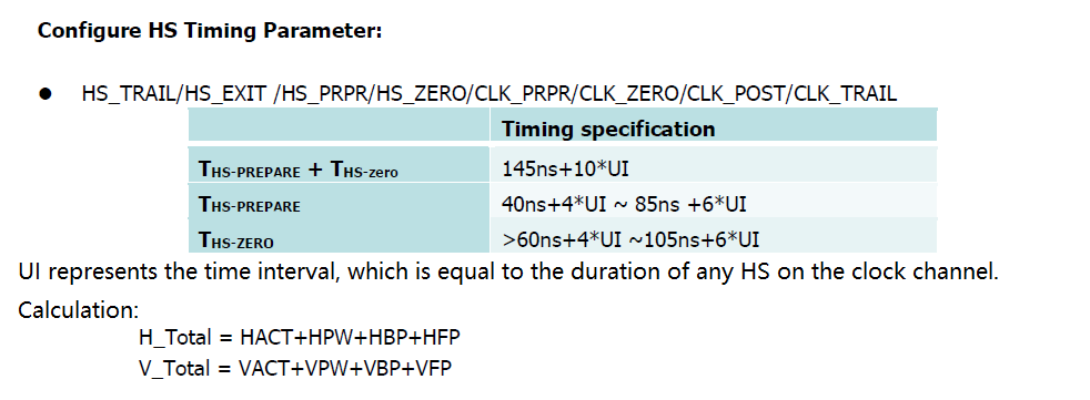
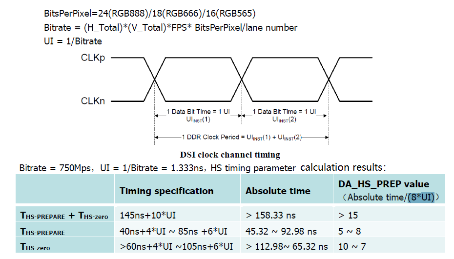
How to configure HS timing parameter.

-
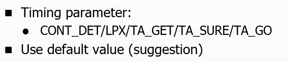
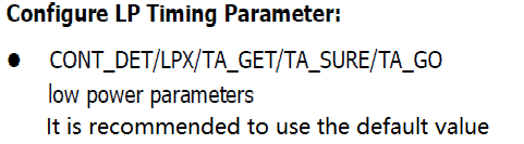
How to configure LP timing parameters
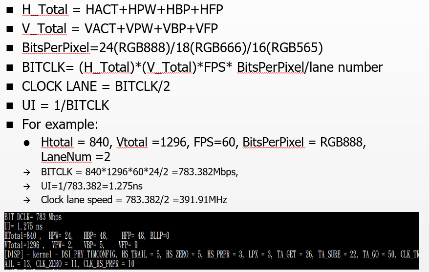
MIPI related parameter calculation table
-
After panel parameter setting, and before program running, check whether the relevant registers and GPIO are set correctly. Such as the customer`s panel lighted by ttl, confirm the /config/riu_w 101e 0xd 0x1000 pin demux settings are correct first, then following gpio required to set to high according to hardware, and different hardware, different settings.
echo 4 > /sys/class/gpio/export
echo out > /sys/class/gpio/gpio4/direction
echo 1 > /sys/class/gpio/gpio4/value
echo 19 > /sys/class/gpio/export
echo out > /sys/class/gpio/gpio19/direction
echo 1 > /sys/class/gpio/gpio19/value
echo 10 > /sys/class/gpio/export
echo out > /sys/class/gpio/gpio10/direction
echo 1 > /sys/class/gpio/gpio10/value
-
Run demo to check whether the screen is normal.
-
After that, close the test pattern and remove the external crystal oscillator of GM to check whether it is ok. Note that the MIPI clock is adjusted correctly:
Pixel CLK: Pixel clock
MIPI CLK: MIPI clock
LVDS CLK: LVDS clock
The calculation formula of pixel clock is:
Pixel CLK=(H Total * V Total) * FPS
The calculation formula of MIPI clock is determined according to the number of LANEs used for MIPI data input.
Mipiclock = [ (width+hsync+hfp+hbp) x (height+vsync+vfp+vbp) ] x(bus_width) x fps/ (lane_num)/2。
The transmission clock frequency of MIPI panel(CLKN,CLKP) is equal to the width of panel resolution(width+hsync+hfp+hbp)x the height of panel resolution(height+vsync+vfp+vbp) x(RGB displayed data width) x frame rate/ (lane_num)/2。
The division by 2 is because MIPI clock is double-edge trigger.
GM8775C, LVDS pixel clock at the output: Pixel CLK=(H Total * V Total) * FPS
For LVDS CLK, when the output is a single-channel LVDS signal, it is equal to its pixel clock. When the output is a dual-channel LVDS signal, it is half of its pixel clock.

-
For the customer`s panel with 960X1280 resolution, set stPanelParam.u16HStart and stPanelParam.u16VStart to 0 to sovle the screen flicker during actual debugging.
-